Multiscale Modeling
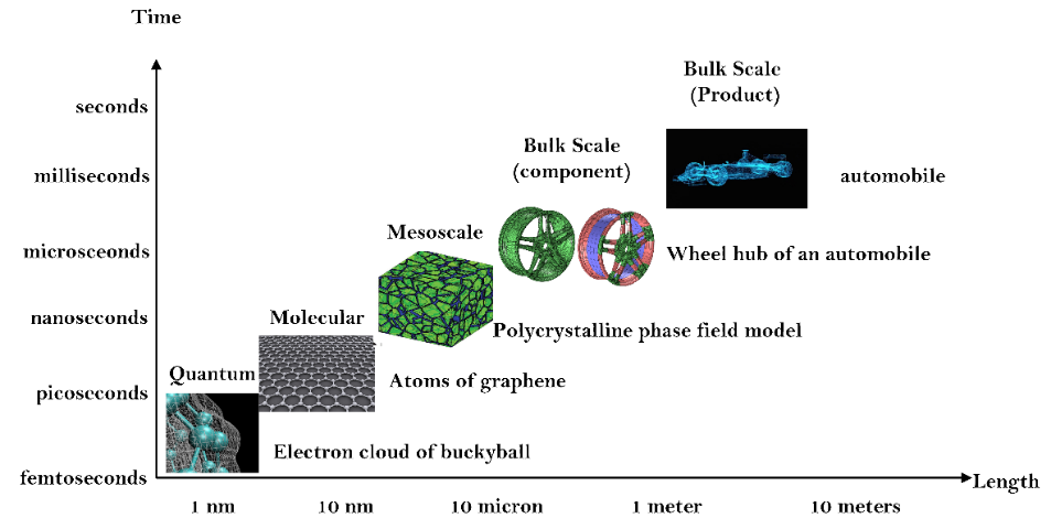
Computational modeling and theoretical prediction play an essential role in designing experiments and determining material properties. The smallest length scale, which corresponds to a few angstroms, is the electronic scale. At the electronic scale, the electron-electron and the nuclei-electron interactions are vital. Here, the system’s total energy is derived by solving the computationally intensive Schrödinger equation of quantum mechanics. Using the current computational architecture, systems with only a few tens of electrons can be simulated by solving the Schrödinger equation. Density functional theory (DFT), which can describe the properties at the ground state of a quantum mechanical system with the knowledge of the density of electrons in real space, it is now possible to study systems at least with few thousands of electrons. The results from DFT calculations can provide accurate information about the properties of crystalline materials.
However, simulating the non-crystalline materials or crystalline materials with varying defect concentrations using DFT is computationally intensive. A better workaround is the hierarchical multiscaling between the electronic and atomic-scale by developing suitable interatomic potentials. At the atomic scale, molecular dynamics simulations with bond order potential that can accurately capture bond breakages have been used to capture the deformation mechanism. Hence in the current thesis, computational simulation of 2D materials such as 2D-hBN and graphene with varying defect densities were simulated using electronic scale DFT and atomic-scale MD, probing their electronic and mechanical properties. Multiple scales of length and time and the relevant theories applicable are illustrated in Figure 1
2D Materials
Introduction
In 2D materials, the third dimension in restricted forming a layered structure of thickness in the nanoscale range. are applicable in many fields due to their unique properties. A few of them are Semiconductors, Energy harvesting, Transparent electrodes, Membranes for atomic separation, Polymer composites (filler materials), Drug delivery(With amine functionalization), Coatings (Surface Engineering). A comprehensive list of the observed property and the corresponding applications is listed in Table 1.
Table 1: Properties observed in graphene and 2D-hBN and their respective applications.
| Graphene (Observed Property) | Application | References |
|---|---|---|
| Large thermal conductivity (5000 W/mK) | Thermal cloaking, Heat dissipaters in High power density devices. | 1–3 |
| Ultra-High strength (YM 1TPa, UTS ~135 GPa) | Filler material in nanocomposites, space applications | 4–6 |
| Exhibits Magnetoresistance | Spintronics | 7 |
| Supercapacitance | Li-Ion batteries, fuel cells, solar cells | 8 |
| 2D hBN (Observed property) | ||
| Wide gap semiconducting material (Insulator) | Laser devices due to bandgap in the UV region | 9–11 |
| High meting point 3400 K | Used in a wide range of high temperature and high-pressure applications | 12 |
| Good Interface properties | Quantum computing | 13 |
| Cytocompatable and bioactive | Capable of mimicking bone collagen fiber | 14 |
Defects in the nanoscale are common in the 2D materials irrespective of the fabricated method. Material performance gets significantly affected due to the presence of defects in 2D materials. Table 2: Topics worked on the current study.
| S.No. | 2D Materials Topics |
| 1. | Electronic and Atomistic scale properties of pristine and defected 2D-hBN |
| 2. | Atomistic scale defect guided deformation mechanism, and mechanical properties of graphene using ReaxFF. |
In the present study (Topic 1 in Table 2), the electronic and mechanical properties of graphene, stanene, 2D hexagonal boron nitride (hBN), are investigated. At the electronic scale, the formation energies, band structures were obtained. At the atomistic level, stiffness, ultimate tensile strength, and fracture strain were simulated for the pristine and defected 2D materials.
2D hBN is simulated at the electronic scale and atomistic scale. At the electronic scale, the formation energies, band structures were obtained for pristine and defected hBN. The substitutional defects of carbon (C-at-NS, C-at-BS), and oxygen (O-at-NS, O-at-BS) at boron and nitrogen sites, single vacancy defects (BV, NV) and triangular vacancies (3B+N)v, (3N+B)v of boron and nitrogen, and Stone Thrower Wales (STW) type-1 & 2 defects were considered. It is found that with the inclusion of defects in 2D-hBN, the bandgap decreases, and carbon substitution at the boron site produces n-type characteristics, whereas substitution of carbon at the nitrogen site produces p-type characteristics. Boron vacancies increased the p-type character. At the atomistic scale, stiffness, ultimate tensile strength, and fracture strain were simulated for the pristine and defected hBN with molecular dynamics (MD) simulations using Tersoff potential. It is also found that the vacancy defects dominated by Boron atoms are energetically favorable and shift the electric conductivity from insulating to conducting. The stiffness and ultimate tensile strain of the 2D-hBN in the zigzag direction are higher than that of armchair direction. A strength reduction of around ~50% is observed with a defect concentration of 2.1%. It is observed that pristine and defective 2D-hBN, is stronger in ZZ than AC configuration. A short illustration of the obtained results are illustrated in Figure 1
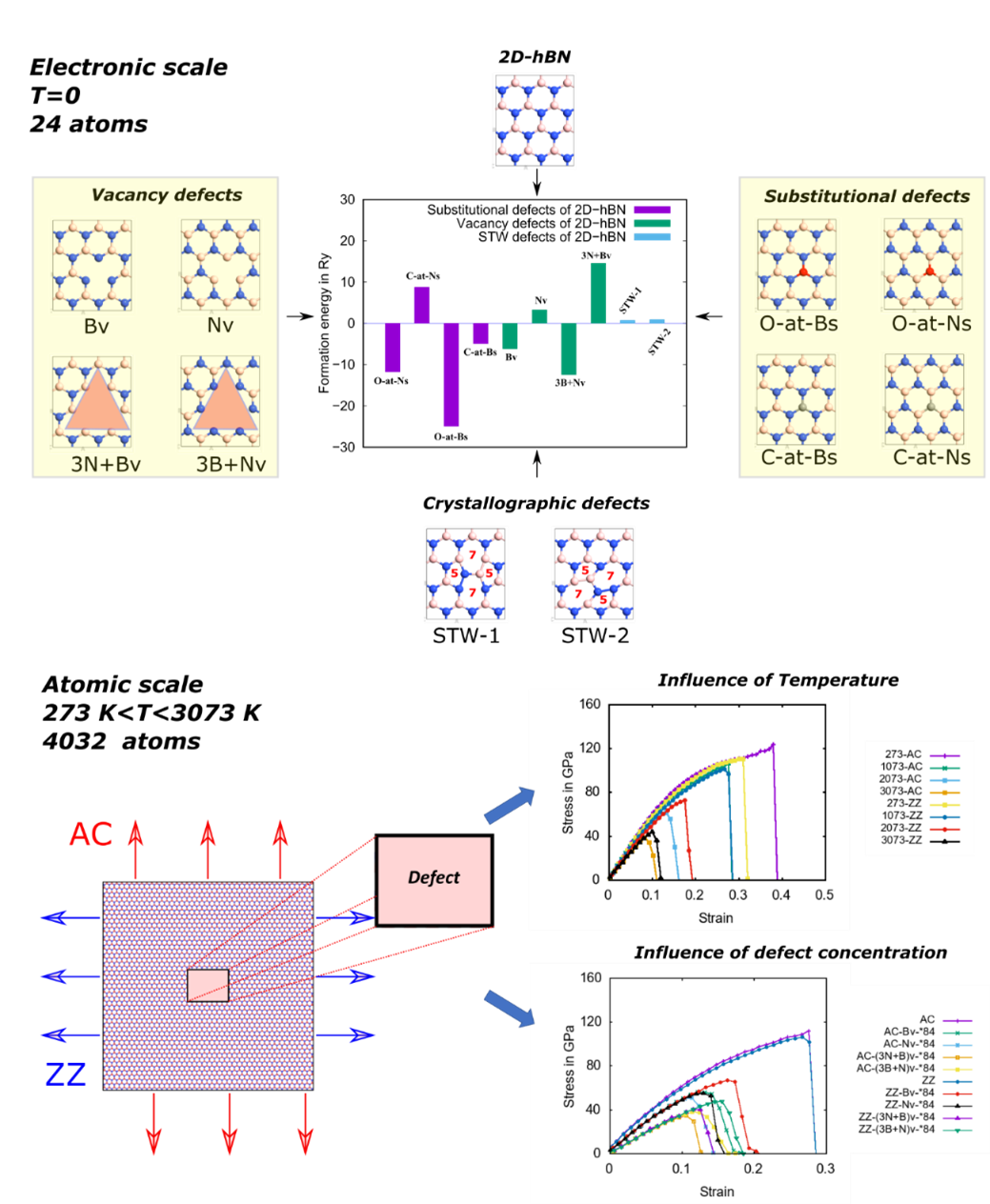
Figure 2: Effect of substitutional and vacancy defects on the electrical and mechanical properties of 2D-hexagonal boron nitride
In the second study (Topic 2 in Table 2) the mechanical properties and failure behavior of graphene were investigated using molecular dynamics. Atomically reactive force field potential, ReaxFF, was used to capture the bond interactions. The nanoscale mechanical properties and failure behavior of graphene with Stone-Wales defect concentration were investigated using molecular dynamics simulations with the latest ReaxFFC-2013 potential that can accurately capture bond breakages of graphitic compounds. The choice of interatomic potential plays an essential role in capturing the deformation mechanism accurately. Stable configuration of two-dimensional graphene experiences out-of-plane deformation leading to ripples and wrinkles in graphene. It is observed that the mechanical properties such as Young’s modulus, ultimate tensile strength, and the fracture strain are dependent on the out-of-plane deformation, temperature, defect concentration, defect orientation, defect layout and loading configuration.
a) b)
c) d) Figure 2: A)Pristine graphene and b) Graphene with varying defect density and defect distribution. C) Stress-strain behaviour of pristine graphene, d) Young’s modulus with varying defect concentrations.
ICME of Metals
Major References:
- Balandin, A. A.; Ghosh, S.; Bao, W.; Calizo, I.; Teweldebrhan, D.; Miao, F.; Lau, C. N. Superior Thermal Conductivity of Single-Layer Graphene. Nano Lett. 2008, 8 (3), 902–907. https://doi.org/10.1021/nl0731872.
- Liu, W.; Li, H.; Xu, C.; Khatami, Y.; Banerjee, K. Synthesis of High-Quality Monolayer and Bilayer Graphene on Copper Using Chemical Vapor Deposition. Carbon 2011, 49 (13), 4122–4130. https://doi.org/10.1016/j.carbon.2011.05.047.
- Klemens, P. G.; Pedraza, D. F. Thermal Conductivity of Graphite in the Basal Plane. Carbon 1994, 32 (4), 735–741. https://doi.org/10.1016/0008-6223(94)90096-5.
- Akinwande, D.; Brennan, C. J.; Bunch, J. S.; Egberts, P.; Felts, J. R.; Gao, H.; Huang, R.; Kim, J. S.; Li, T.; Li, Y.; Liechti, K. M.; Lu, N.; Park, H. S.; Reed, E. J.; Wang, P.; Yakobson, B. I.; Zhang, T.; Zhang, Y. W.; Zhou, Y.; Zhu, Y. A Review on Mechanics and Mechanical Properties of 2D Materials—Graphene and Beyond. Extreme Mechanics Letters. 2017. https://doi.org/10.1016/j.eml.2017.01.008.
- Siochi, E. J. Graphene in the Sky and Beyond. Nat. Nanotechnol. 2014, 9 (10), 745–747. https://doi.org/10.1038/nnano.2014.231.
- Wei, Y.; Yang, R. Nanomechanics of Graphene. Natl. Sci. Rev. 2019, 6 (2), 324–348. https://doi.org/10.1093/nsr/nwy067.
- Han, W.; Kawakami, R. K.; Gmitra, M.; Fabian, J. Graphene Spintronics. Nature Nanotechnology. 2014. https://doi.org/10.1038/nnano.2014.214.
- Wang, H.; Cui, L.-F.; Yang, Y.; Sanchez Casalongue, H.; Robinson, J. T.; Liang, Y.; Cui, Y.; Dai, H. Mn3O4-Graphene Hybrid as a High Capacity Anode Material for Lithium Ion Batteries. J. Am. Chem. Soc. 2010, 132, 13978–13980. https://doi.org/10.1021/cm101532x.(9).
- Topsakal, M.; Aktürk, E.; Ciraci, S. First-Principles Study of Two- and One-Dimensional Honeycomb Structures of Boron Nitride. Phys. Rev. B - Condens. Matter Mater. Phys. 2009, 79 (11), 1–11. https://doi.org/10.1103/PhysRevB.79.115442.
- McDougall, N. L.; Nicholls, R. J.; Partridge, J. G.; McCulloch, D. G. The near Edge Structure of Hexagonal Boron Nitride. Microsc. Microanal. 2014, 20 (4), 1053–1059. https://doi.org/10.1017/S1431927614000737.
- Watanabe, K.; Taniguchi, T.; Kanda, H. Direct-Bandgap Properties and Evidence for Ultraviolet Lasing of Hexagonal Boron Nitride Single Crystal. Nat. Mater. 2004, 3 (6), 404–409. https://doi.org/10.1038/nmat1134.
- Eichler, J.; Lesniak, C. Boron Nitride (BN) and BN Composites for High-Temperature Applications. J. Eur. Ceram. Soc. 2008, 28 (5), 1105–1109. https://doi.org/10.1016/j.jeurceramsoc.2007.09.005.
- Zhang, Y. G.; Cheng, G. D.; Peng, W.; Tang, Z. Spintronic and Electronic Properties of a Positively Charged N BVN Center in Hexagonal Boron Nitride Monolayer. Comput. Mater. Sci. 2014, 95, 316–319. https://doi.org/10.1016/j.commatsci.2014.08.003.
- Horváth, L.; Magrez, A.; Golberg, D.; Zhi, C.; Bando, Y.; Smajda, R.; Horváth, E.; Forró, L.; Schwaller, B. In Vitro Investigation of the Cellular Toxicity of Boron Nitride Nanotubes. ACS Nano 2011, 5 (5), 3800–3810. https://doi.org/10.1021/nn200139h.